
You can now get chips called PLA (programmable logic arrays) and "program" them to implement Boolean functions. I'll explain what it means to program a PLA.
Fortunately, a PLA is quite simple to learn, and produces nice neat circuits too.
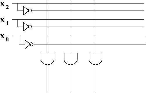
Each variable is hooked to a wire, and to a wire with a NOT gate. So the top wire is x2 and the one just below is its negation, \x2.
Then there's x1 and just below it, its negation, \x1.
The next part is to draw a vertical wire with an AND gate. I've drawn 3 of them.
Let's try to implement a truth table with a PLA.
| x2 | x1 | x0 | z1 | z0 |
| 0 | 0 | 0 | 0 | 0 |
| 0 | 0 | 1 | 1 | 0 |
| 0 | 1 | 0 | 0 | 0 |
| 0 | 1 | 1 | 1 | 0 |
| 1 | 0 | 0 | 1 | 1 |
| 1 | 0 | 1 | 0 | 0 |
| 1 | 1 | 0 | 0 | 0 |
| 1 | 1 | 1 | 0 | 1 |
Each of the vertical lines with an AND gate corresponds to a minterm. For example, the first AND gate (on the left) is the minterm: \x2\x1x0.
The second AND gate (from the left) is the minterm: \x2x1x0.
The third AND gate (from the left) is the minterm: x2\x1\x0.
I've added a fourth AND gate which is the minterm: x2x1x0.
The first three minterms are used to implement z1. The third and fourth minterm are used to implement z0.
This is how the PLA looks after we have all four minterms.

Now you might complain. How is it possible to have a one input AND gate? How can three inputs be hooked to the same wire to an AND gate? Isn't that invalid for combinational logic circuits?
That's true, it is invalid. However, the diagram is merely a simplification. I've drawn the each of AND gate with three input wires, which is what it is in reality (there is as many input wires as variables). For each connection (shown with a black dot), there's really a separate wire. We draw one wire just to make it look neat.

The vertical wires are called the AND plane. We often leave out the AND gates to make it even easier to draw.
We then add OR gates using horizontal wires, to connect the minterms together.

Again, a single wire into the OR gate is really 4 wires. We use the same simplification to make it easier to read.
The horizontal wires make up the OR plane.
This is how the PLA looks when we leave out the AND gates and the OR gates. It's not that the AND gates and OR gates aren't there---they are, but they've been left out to make the PLA even easier to draw.

You can generally get around the problem by not connecting the wire to each of the three variables. For example, you could just have a product term x2\x0 or even simply \x1.
For the purpose of implementing truth tables, we'll usually tell you not to simplify, and to let each vertical line be a minterm.